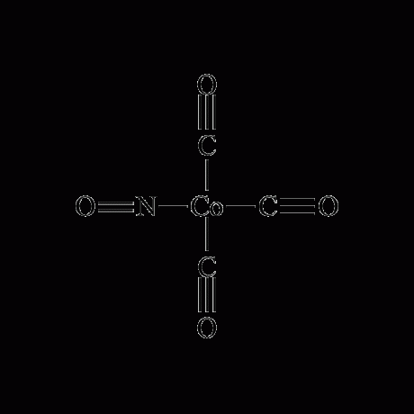
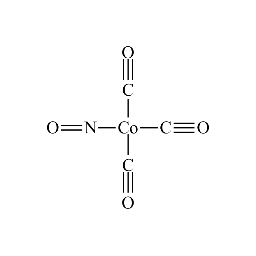
Cobalt Tricarbonyl Nitrosyl
| SKU | Name | Molecular Weight | Melting Point (°C) | Boiling Point (°C / mm Hg) | Vapor_Pressure_1_mm | Density | Ionization Energy (ev) |
|---|---|---|---|---|---|---|---|
| INCO032 | COBALT TRICARBONYL NITROSYL | 172.97 | -1.1° | 50 | -- | 1.47 | -- |
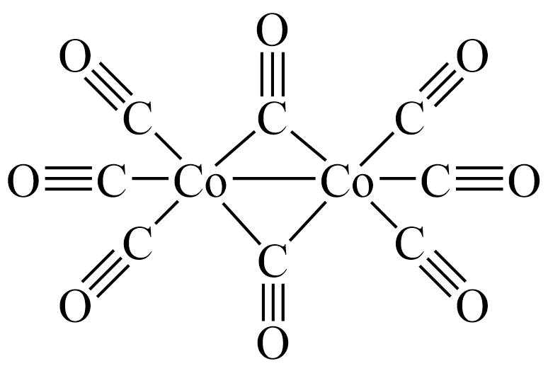
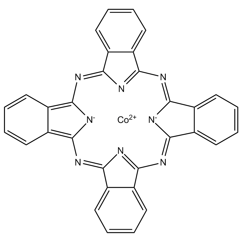
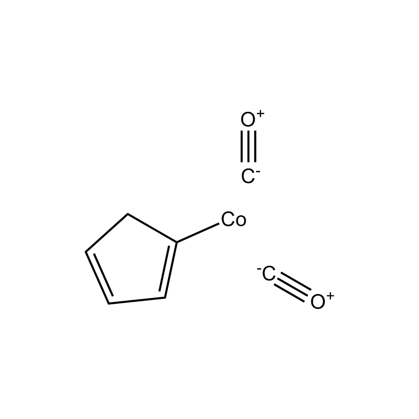
Cobalt tricarbonyl nitrosyl presents clear advantages versus other available precursors in CVD deposition processes. Cobalt tricarbonyl nitrosyl is a liquid, in contrast to most Co precursors which are solids. Further, thermal decomposition of cobalt carbonyl [Co2(CO)8] introduces undesirable reaction products (polymerization products together with HCo(CO)4 arising from H2 available in the chamber), and is not very stable under normal storage conditions. Other precursors for Co CVD include cobaltocene [Co(C5H5)2], cyclopentadienylcobalt dicarbonyl [C5H5Co(CO)2], and cobalt acetylacetonate [Co(C5H7O2)3]: all these sources require H2 reduction and under atmospheric pressure CVD (APCVD) yield Co films with an unacceptably rough surface morphology.
Cobalt tricarbonyl nitrosyl has high volatility (vapor pressure 26 Torr at 0 °C and 100 Torr at 25 °C), is available in liquid form, and exhibits good stability (decomposition temperature >66 °C) and low toxicity. Furthermore, Co is in an oxidation state of zero in this compound, which implies that metal-ligand bonds are easily cleaved to yield pure metal films, and only CO + NO as byproducts.
Applications:
- Deposition of cobalt for magnetic thin films (Deo, N. et al. Journal of Material Science 2005, 347-392.)
- In combination with Fe(CO)5 forms spherical Fe/Co particles (Morita, H. et al. J. Photochem. Photobiol., A 2009, 206, 205.)
- Low Temperature CVD methodology of epitaxial CoSi2 growth (Londergan, A et al. Journal of the Electrochemical Society 2001, 148 C21-C27. AE Kaloyeros, A Londergan, B Arkles – US Patent 6,346,477, 2002.)
- Employed in CVD of cobalt and epitaxy formation of cobalt silicide (Ivanova, A. et al. J. Electrochem. Soc. 1999, 146, 2139.)
- Optimize processing Co epitaxy growth in integrated silicide circuits (Ivanova, A et al. Journal of the Electrochemical Society 1999, 146 2139-2145.)
- Forming electrical contacts on transistor source/drain and gate regions (Ishizaka, T. et al. – US Patent 8372739, 2013.)
The growth of thin films via chemical vapor deposition (CVD) is an industrially significant process with a wide array of applications, notably in microelectronic device fabrication. Chemical vapor deposition (CVD) is carried out by passing a volatilized precursor (such as a silane, organometallic or metal coordination complex) over a heated substrate. Thermal decomposition of the precursor produces a thin-film deposit, and ideally, the ligands associated with the precursor are cleanly lost to the gas phase as reaction products. Compared to other thin-film production techniques, CVD offers several significant advantages, most notably the potential for effecting selective deposition and lower processing temperatures. Many metal CVD depositions are autocatalytic. Growth of such thin films is characterized by an induction period, which is a consequence of the higher barriers that relate to the activation of the precursor on a non-native substrate. CVD is the preferred deposition method for fabricating optical storage, as it is a well established method with good scalability, reproducibility, and uniformity. It is also capable of high rates and good composition control.


